A piezo element is a ceramic that expands or contracts when an electrical charge is applied, generating linear movement and force. Multiple piezo elements can be layered on top of each other, creating what is known as a stacked piezo actuator. These devices take advantage of the combined effect of each element’s expansion to produce a useful movement and force.
Displacement
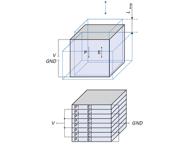
Individual piezo elements in a stacked actuator have alternating polarity, and the electrical field is applied parallel to the direction of polarization. When a voltage is applied, a strain, or displacement, is induced in the direction of polarization. The movement of a piezo element equals the amount of voltage applied multiplied by the piezo electric coefficient. (The piezo electric coefficient, d33, relates to the material’s efficiency in transferring electrical energy to mechanical energy.) Because they are connected mechanically in series, the total movement of a stacked piezo actuator is the product of a single element’s movement, times the number of elements in the stack.
ΔL = n * d33 * V
ΔL = change in length (m)
n = number of piezo layers
d33 = longitudinal piezo electric coefficient (m/V)
V = operating voltage (V)
The total displacement of a stacked actuator is generally between 0.1 and 0.15 percent of the actuator length.

Image credit: PI Ceramic GmbH
Voltage and Electric Field
Stacked piezo actuators are generally classified as either low voltage (below 200 V) or high voltage (up to 1000 V), referring to the maximum input voltage for maximum stroke. The amount of voltage that can be applied is determined by the material and the thickness of each element. The relationship between the electrical field and the driving voltage is given by the equation:
E = V/th
E = electric field (V/m)
V = applied voltage (V)
th = thickness of one piezo layer (m)
Thus, the electric field increases as the layer thickness decreases. Similarly, for a given electrical field, the driving voltage must decrease as the layer thickness decreases.
Force and Stiffness
Actuator stiffness has a significant influence on force generation, and is determined by the modulus of elasticity of the piezo ceramic material, the actuator’s cross-sectional area, and its length.
kA = (E*A) / l
kA = actuator stiffness (N/m)
E = modulus of elasticity (N/m2)
A = actuator cross-sectional area (m2)
l = actuator length (m)
Despite their small size, stacked piezo actuators have a force density in the range of 30 N/mm2, which allows them to produce useful forces in the tens of thousands of Newtons. It’s important to note that in steady state operation (no movement, constant force), no current is flowing and no power is required. Stacked actuators are also able to hold their position when power is off, and can do so without generating heat.
Tensile Strength and Preload
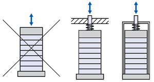
Stacked piezo actuators often see both compressive and tensile forces, especially during highly dynamic movements. The tensile strength of a stacked actuator is largely determined by the method used to laminate the individual elements together, and is generally an order of magnitude lower than the compressive strength. Preloading the actuator to a value greater than the applied tensile load will ensure that the actuator always stays in compression and can operate in highly dynamic, bi-directional applications. Successful integration of a stacked piezo actuator requires that any applied forces be axial and compressive only. Manufacturers typically offer a variety of mounting options to help prevent bending, shear, or torsional forces.

Image credit: PI Ceramic GmbH
Applications
Piezo actuators directly convert electrical energy to mechanical energy through the piezoelectric effect, meaning they have no moving parts that generate friction or wear. Thus, their resolution is limited only by external mechanical and electrical components. They can achieve extremely fast response times and high acceleration rates, which makes them especially useful for sinusoidal operation. Stacked piezo actuators are capable of operating in environments such as vacuum, cryogenic conditions, and the presence of magnetic fields, making them suitable for applications in the consumer electronics, aerospace, automotive, and semiconductor industries.
Feature image credit: PI Ceramic GmbH


Leave a Reply
You must be logged in to post a comment.